


Characterization Laboratory
 Aim:
Aim:
SEM laboratory was established to investigate surface morphologies of metallic and non-metallic materials at high magnification and resolution as well as to determine spatial distribution and the amounts of chemical elements (Be-U) in those materials. In addition to failure analysis, microstructure observation of new products is also the aim of this laboratory.
Services
Analyses and Tests
- Coating of non-metallic materials with Au-Pd and C to make them conductive,
- Imaging the surface morphologies of metallic and non-metallic materials by using secondary electrons (SE method),
- Imaging the distribution of light and heavy elements in metallic and non-metallic materials by using back-scattered electrons (BE method),
- Conducting qualitative and semi-quantitative chemical analyses of materials by the EDS method ),
- Providing EDS results in the form of point, line, area analyses and x-ray mapping,
Analyzes Used in Scientific Research Activities
- Coating of non-metallic materials with Au-Pd and C to make them conductive,
- Imaging the surface morphologies of metallic and non-metallic materials by using secondary electrons (SE method),
- Imaging the distribution of light and heavy elements in metallic and non-metallic materials by using back-scattered electrons (BE method),
- Conducting qualitative and semi-quantitative chemical analyses of materials by the EDS method ),
- Providing EDS results in the form of point, line, area analyses and x-ray mapping,
Laboratory Infrastructure
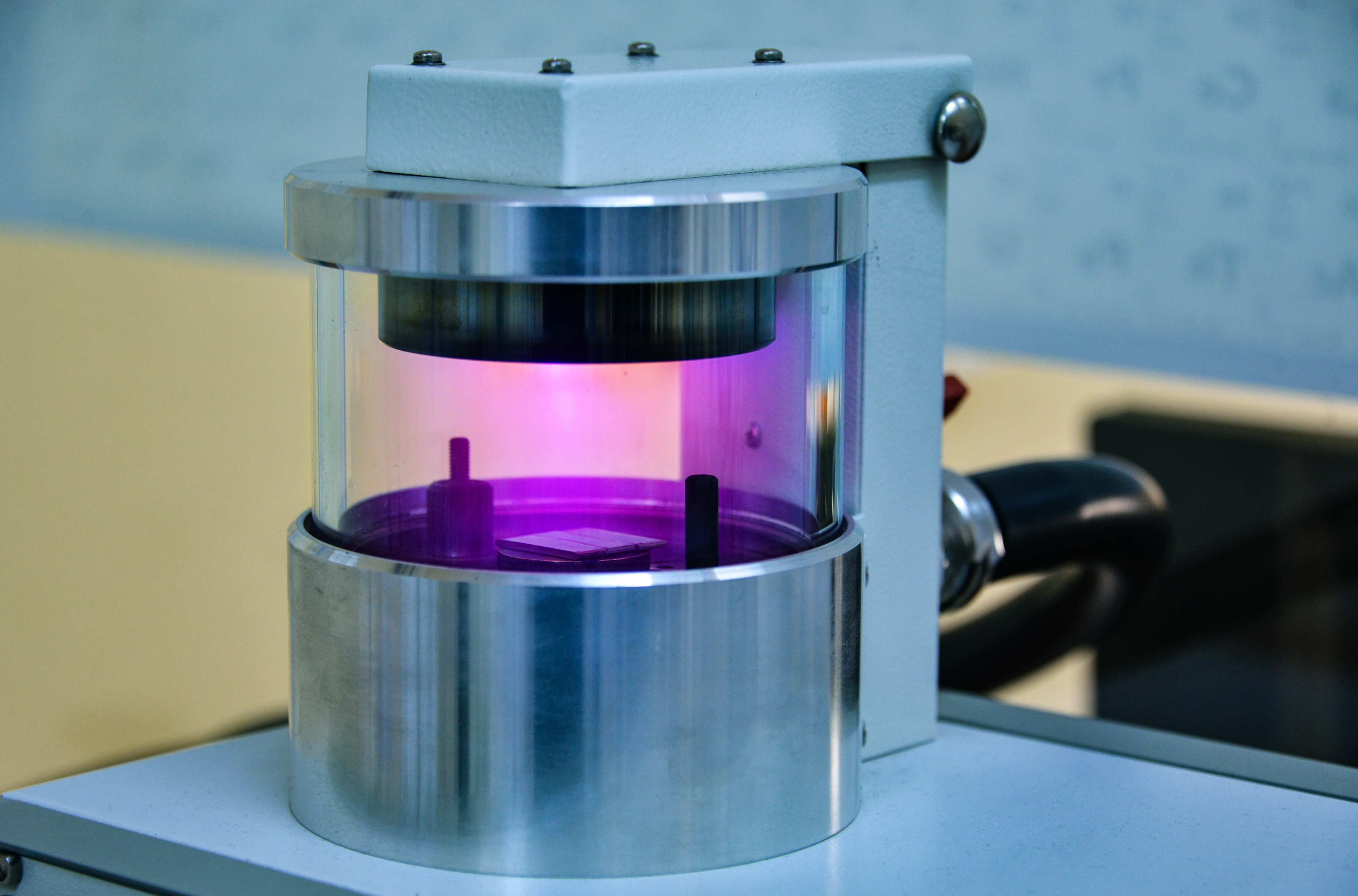
- Au-Pd Coating System
- C Coating System
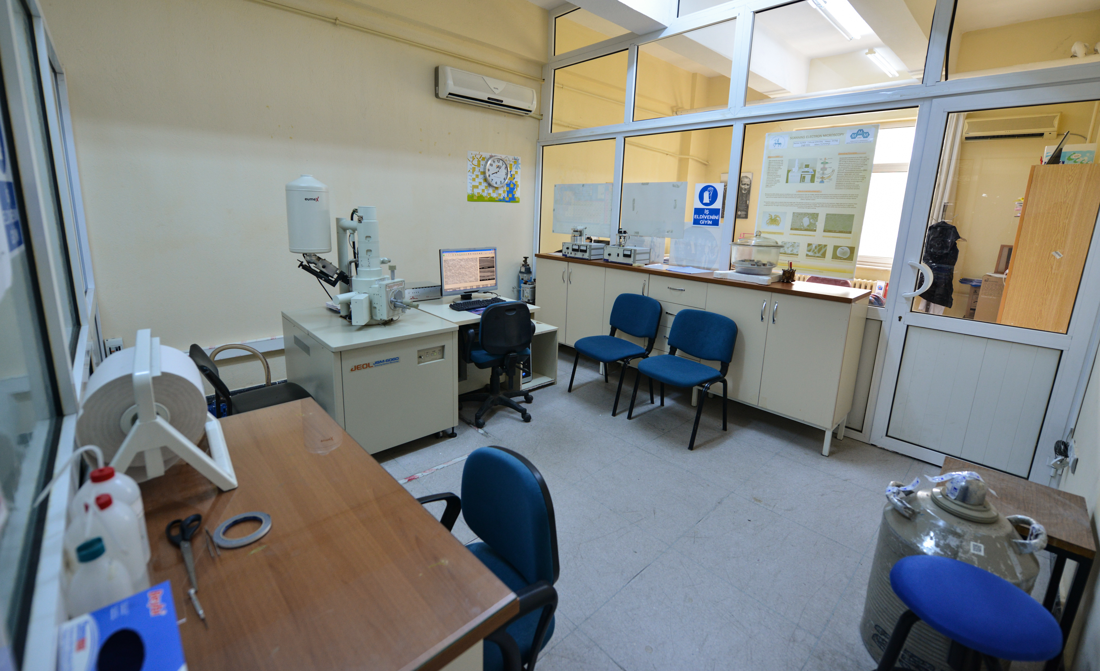
- Scanning Electron Microscope (SEM) and Energy Dispersive Spectrometer (EDS)
Laboratory Images

Team
Assoc. Prof. Esra DOKUMACI ALKAN
Contact
Department of Metallurgical and Materials Engineering